


In a significant boost to India's rapidly expanding semiconductor ecosystem, D. Sridhar Babu (Telangana Minister for Information Technology, Electronics, Communications, Industries and Commerce) inaugurated the country's first Chemical Mechanical Planarization (CMP) Pad Technology Hub in Hyderabad. This is the first step toward building a domestic semiconductor manufacturing facility for the country and reducing reliance on imported high-precision materials used in chip production.
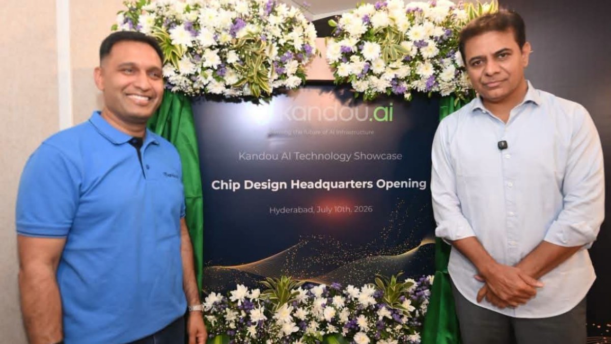
The inauguration is an example of Telangana’s rise as a technology and innovation hub in advanced electronics, semiconductor manufacturing, research and development and precision engineering. In the last few years Hyderabad has become one of India’s leading technology centers and has attracted world-class companies in electronics manufacturing, semiconductor design, artificial intelligence, aerospace, biotechnology, and data centres.
CMP pads are one of the most important consumables in semiconductor manufacturing. In the chip fabrication process, Chemical Mechanical Planarization is used to smooth and polish silicon wafers, creating a flat surface before more layers of tiny electronic circuits are added. This polishing process is crucial for building advanced integrated circuits in smartphones, computers, automobiles, medical equipment, telecommunications infrastructure, artificial intelligence systems, etc.
The new technology hub launched will contribute to the research, product development, testing and manufacturing of CMP pad technologies in India. Until now, much of the country's requirement for such high-end consumables for semiconductor use has been imported by international suppliers. Developing indigenous capabilities in this area is viewed as an essential step toward a robust semiconductor supply chain.
In the inauguration, Minister Sridhar Babu said Telangana is committed to developing advanced manufacturing and innovation. He said the CMP Pad Technology Hub is in alignment with the state’s industrial vision and the government’s vision to create a globally competitive semiconductor ecosystem through development of innovative technologies and self-reliance from a technological perspective.

Semiconductor manufacturing depends not only on state-of-the-art fabrication plants but also on a large number of suppliers producing special equipment, chemicals and high-tech components. Facilities like the CMP Pad Technology Hub provide critical supporting infrastructure to support the semiconductor industry’s growth.
The hub will also promote collaboration between industry, academic institutions, research organizations and technology startups. Such partnerships can speed up the development of material science, precision engineering, nanotechnology and semiconductor process technologies and create new opportunities for indigenous product development.
Hyderabad’s well-established research ecosystem, highly trained engineers and good colleges make it a perfect place for advanced semiconductor research. The new facility could attract further investment from domestic and international technology companies looking to set up manufacturing and research centers in India.
The technology hub will, in addition to boosting industrial capacity, also generate job opportunities for high-skilled engineering, research, quality assurance, materials science, manufacturing, and technical services. The semiconductor industry is now one of the world’s fastest-growing industries, and good job prospects are there for engineers, scientists and skilled technicians.
The launch also fits squarely into India’s wider semiconductor mission to develop domestic manufacturing capacity, encourage research and innovation, and reduce reliance on global supply chains for critical technologies. As semiconductor chips play an increasingly important role in electric vehicles, consumer electronics, healthcare, telecommunications, defence, renewable energy and industrial automation, the investments in supporting technologies like CMP pads are equally significant.
Industry analysts argue that local knowledge in semiconductor consumables enhances India's competitive position in the supply chain, can reduce production costs over time and enhances the technological capabilities of Indian companies.
The CMP Pad Technology Hub is expected to be a place of innovation, product validation, process optimization and workforce development to bridge existing gaps in the semiconductor manufacturing ecosystem in India. Researchers and engineers at the facility will likely be working on polishing materials that are of a high quality that are suitable for modern semiconductor fabrication plants.
As India expands its semiconductor business outlook, projects like this point to an ever-growing collaboration of government, industry leaders and research institutions. Telangana’s proactive approach to attracting technology investments has only strengthened Hyderabad's reputation as one of the country’s leading centres for advanced manufacturing and innovation.
For India, the launch of the first CMP Pad Technology Hub is more than just a new facility but also a symbol to support the country's development in the semiconductor industry, and to be a technology player in the future. By investing in dedicated manufacturing capabilities, research infrastructure, and skilled personnel, India is already in the process to become a significant global player in the semiconductor industry.