


One of South Korea’s leading semiconductor companies, Seoul Semiconductor, is in talks with the governments of Tamil Nadu, Karnataka and Gujarat to establish an Assembly, Testing, Marking and Packaging (ATMP) facility for optoelectronic semiconductor products in India. The investment in the construction of an assembly, testing, marking and packaging (ATMP) facility indicates that global semiconductor companies are looking to enter India to become an electronics manufacturing hub and that the country’s goal is to become a major global semiconductor center.
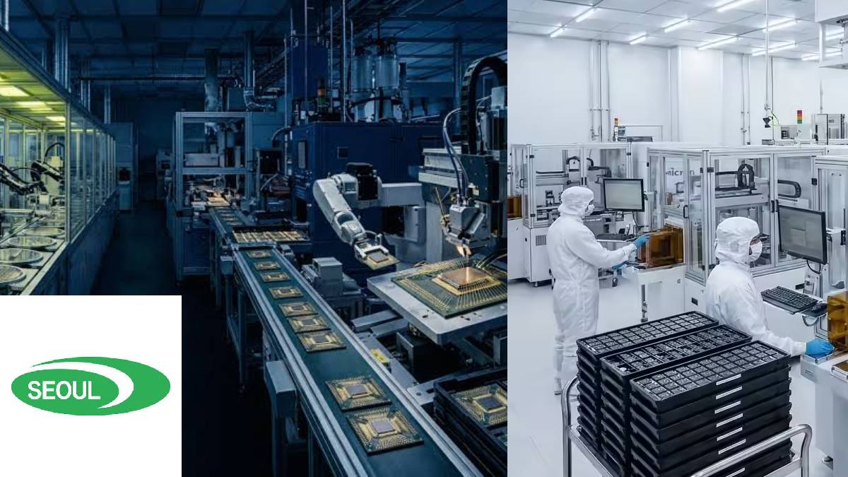
The proposed ATMP facility would be at the center of the assembly, testing, marking, and packaging of optoelectronic semiconductor devices, which are commonly used in LED lighting, automotive systems, consumer electronics, display technologies, industrial equipment, healthcare devices, and communication systems. Such a facility would strengthen India's semiconductor value chain and reduce dependence on imported semiconductor components.
India is now a popular place for semiconductor investments because of government investment in production-linked incentive (PLI) schemes, semiconductor incentive programs, and efforts to create a comprehensive semiconductor ecosystem. Many international companies have made investments in semiconductor fabrication, chip packaging, and electronics manufacturing in recent years, and India is now in a position to become one of the largest exporters of semiconductors in the global network.
The discussions with Tamil Nadu, Karnataka, and Gujarat demonstrate the tough competition between Indian states for high-value technology investments to attract investments in these states and create a state-level technology ecosystem. Each of these states has developed good industrial ecosystems and has unique strengths in semiconductor manufacturing.
Tamil Nadu is now one of India’s leading electronics manufacturing centers, home to a robust automobile industry, robust industrial infrastructure, a skilled workforce and a developing electronics supply chain. It has been actively promoting investment in semiconductors, advanced manufacturing, and electronic component production.

Karnataka is home to Bengaluru and has a mature technology ecosystem with a strong presence of semiconductor design companies, research institutions, engineers and global technology firms. The innovation-oriented nature of the state makes it a good place to do electronics manufacturing and research.
Gujarat has become a preferred location for semiconductor investments with industrial policy development, infrastructure development, and large-scale semiconductor projects. It has attracted massive investments in semiconductor fabrication and related industries and is projected to become one of the manufacturing hubs in the future.
The optoelectronics ATMP facility would complement India’s larger semiconductor strategy to focus on the backend stages of semiconductor production. In semiconductor fabrication plants, silicon wafers and chips are made, but the ATMP process is crucial for assembling semiconductor dies into packages and testing their functionality, marking finished products, and preparing them for commercial use. These operations are crucial for product quality, reliability, and performance before things get to electronics manufacturers.
Optoelectronic semiconductors play a major role in modern technology. They are used in LED lighting, laser diodes, optical sensors, image sensors, infrared devices, automotive lighting systems, smart displays, fiber-optic communications, and advanced medical equipment. As industries develop electric vehicles, smart infrastructure, artificial intelligence, automation, and energy-efficient technologies, demand for them is rising.
If the project moves forward, it is expected to create high-skilled employment opportunities in engineering, manufacturing, quality assurance, automation, research and development, logistics and supply chain management. It may also encourage the development of local suppliers of semiconductor materials, packaging solutions, testing equipment, and precision manufacturing components.
The investment is in line with India's long-term goals of decreasing import dependence and developing a robust domestic semiconductor ecosystem. Expanding semiconductor packaging and testing capability is one of the key steps in establishing a global semiconductor value chain from the product to the end user.
For Seoul Semiconductor, establishing an ATMP facility in India would give access to one of the world's fastest-growing electronics markets and build an Asian manufacturing base. Local production could increase supply chain efficiency, shorten delivery time, and better serve customers in India and in neighbouring countries.
Though these discussions are not yet completed, Seoul Semiconductor’s interest shows that the country's attractiveness to the region as a place to invest in technology development is increasing, and if we can make it feasible to do that, Seoul Semiconductor will be a great place to invest in, as the expansion of the semiconductor industry (policy support, skilled talent and industrial development) can be a great step forward in making India a leading place for semiconductor manufacturing and innovation around the world.